* * * 50% OFF * * *
FDA-1 PCM1794A DAC clearance Sales and while stock last!
NEW prices in the STORE page.
I have updated a new user manual as below:
FDA-1 PCM1794A DAC clearance Sales and while stock last!
NEW prices in the STORE page.
I have updated a new user manual as below:
I buy this XMOS USB 2.0 reference design evaluation board from Digikey for US$141.91. It can receive USB 2.0 24bit/192k Fs signal and output to SPDIF optical and I2S besides stereo analogy input/output. The board will require firmware programming before it can be used. Details can be found in XMOS website.
Digikey item: 880-1017-ND
.
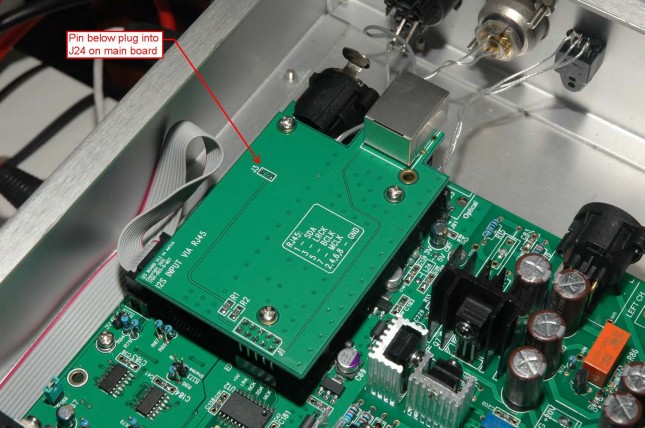
For I2S, the signal is labelled on the board and I use 2.54mm pin header for connection to my PCM1794A DAC board. The USB board use the power from USB connection at about 150mA and thus do not need any outside power supply. The good thing about the reference design board is that XMOS provide all the details of design, schematic, pcb layout and software to make it work in almost any platform that can accept I2S or optical signal.
.
Since I use Windows system and thus I need to install a Thesycon drivers which is also free from XMOS website after registration. The diver works with the USB2.0 reference design boards without any issue but it will beep once every 30mins of use. Overall it is a complete design and easy evaluation of the performance by both industry or DIYers.
.
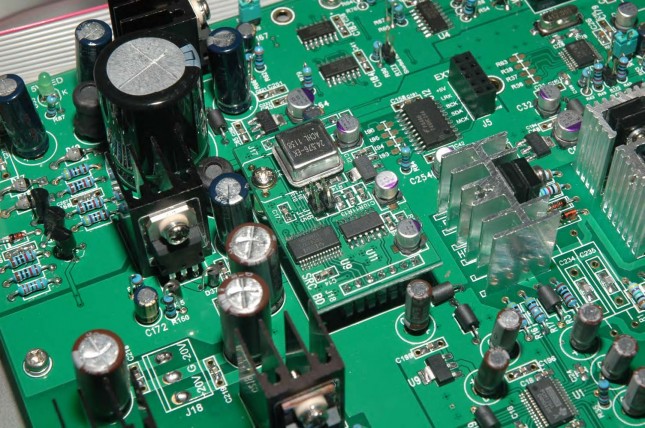
Photo shows how I mount it piggyback on a daughter board and then plug into my DAC main board.
I owned this equipment for few years and got that from ebay Singapore for less than US$500. The equipment label indicated that this machine was from AMD Singapore lab. The condition is excellent as it was seldom used in a smoke free environment. In fact, I want to own a curve tracer long ago because my first job is using Tektronix 576 for discrete part quality control. Tek 577 fit to my needs for its size, weight, price and higher supply voltages till 1600V!
.
Here I use 577 to demo the measurement of jfets 2SK363BL (or 2SK369BL) that I am still selling right now. The horizontal is 5v/div and thus 5 division is about 25V to the middle of the screen. The vertical scale is 2mA/div. Thus you can see the idss value by multiple the div to 2mA easily. In my experience, due to its scale is on the screen with 0.2div resolution, thus the accuracy of the measurement is about 0.2/8 (max number of division) = 2.5%. The top line is Idss, the line below top line is Idss at – 1 div or -0.1V and so on… From the measurement, the Yfs is more than 50mS at about 8mA and this show that the jfet is well within specification.
.
If you observe the curve carefully, and calculate the Yfs using the -0.1V and -0.2V line, you will get a lower Yfs. That means the Yfs decrease with working current (or bias point).
.
Another idea is use this machine to measurement vacumn tube (valve) but a fixture with safety precautions must be built as the it has very high voltage and power up to 100W!!! Take you own risk as I am not liable for that!
HP 1660EP Logic analyzer
I recently acquired this machine for a reasonable price in Singapore. The set did not bootup properly when received due to hard disk failure. After replacing the hard disk, the set is able to power up, passed all performance verification tests and function normally. The model of IBM drive I use is Travelstar DJSA-210 6.0GB. I also tried one Toshiba 6G harddisk but the 1660EP refuse to detect the harddisk. Thus I strongly recomment only IBM brand hard disk should be used.
There are few difficulties in using this old equipment. Firstly is to replace a old hard disk with about 2.1G to 4.3G size. So the only place is to look into old computer shops (local junk yards or ebay). The machine is able to use only 2GB of the hard disk space even if the original size of HD is larger than 2GB (may be OS/firmware limitation). Secondly, the software from hp website has to be loaded into the hard disk from the floopy drive. It is not easy to get diskette and copy the download files onto it. I manage to get a used IBM USB floopy drive for cheap price and NOS box of floopy diskette to complete the job easily. Thirdly, the ROM update has to be done by floopy drive and it is not possible to boot up the machine once the ROM data is erased. Thus do not erase the ROM content if you are not sure if the floopy or floopy drive is working perfectly. Lastly, if the floopy dirve need to be replaced, the source is from some old notebook drive which can be very cheap at scrap cost. Model is Teac FD-05HF and the same model is used in those TDS744 series digital oscilloscopes.
Some photos below:
After a bit study, I install a X-server cygwin on my PC and then I can link the 1660EP X-window to my computer screen. It is not that reliable due to some wild character transfer and breaks the connection.
I have owned this equipment for few years and recently I find that the Digital input from BNC for channel I and II is not working properly. The symptoms are summary as below:
1. Channel I level cannot detect and thus refuse to do any measurement. Channel II can detect signal and do measurment.
2. The 75 ohm and Hi-Z switch is not functioning. For XLR input, the 110 ohm or Hi-Z is able to be selected and hear relay “click”.
3. When Gen Mon is selected, no measurement for both channels.
After checking the signal path of all digital signals using the generator as the digital source, it seems that the circuit is all working fine. On the front panel connector pcb, there is a MAX310 multiplexter to select different input connector and signals. Pin 15, 16 and 17 are address input A0, A1 and A2. In XLR mode, the voltages are solidly at ground level but at BNC mode, the pin A0 is like floating.
After spending hours of tracing the path (It is a multi layer pcb and thus the trace is not on top or bottom and I do not have a service manual of this equipment!) from the connectors of the main board, it was found that the address bus A0 to A3 is connected to an IC 74FCT16374AT – Pin 2, 3 and 5. Since XLR mode is working, thus there is no connection issue for this three pins. Pin 1 of 74FCT16374AT is the Enable pin of these three output address and thus I use a scope probe pin to check on this voltage. When I touch the pin 1, I hear a relay “click” sound and then the measurement of input digital signal is back to normal. When I remove the probe, the issue is back again! After I check connection of pin 1 using multimeter, the pin seems to be not connected to the pad due to dry joint (visually I cannot see any issue!). So the problem is removed after touching up the pin 1 of this IC with some solder paste. Here I attached a photo for those people who may have similar problem as my equipment.
Powered by WordPress