This scope failed 3 years ago and the symptom was just no display after power on but some LEDs flicks to a point and stopped at “ADD” LED there! Recently I take it out and attempt to repair it.
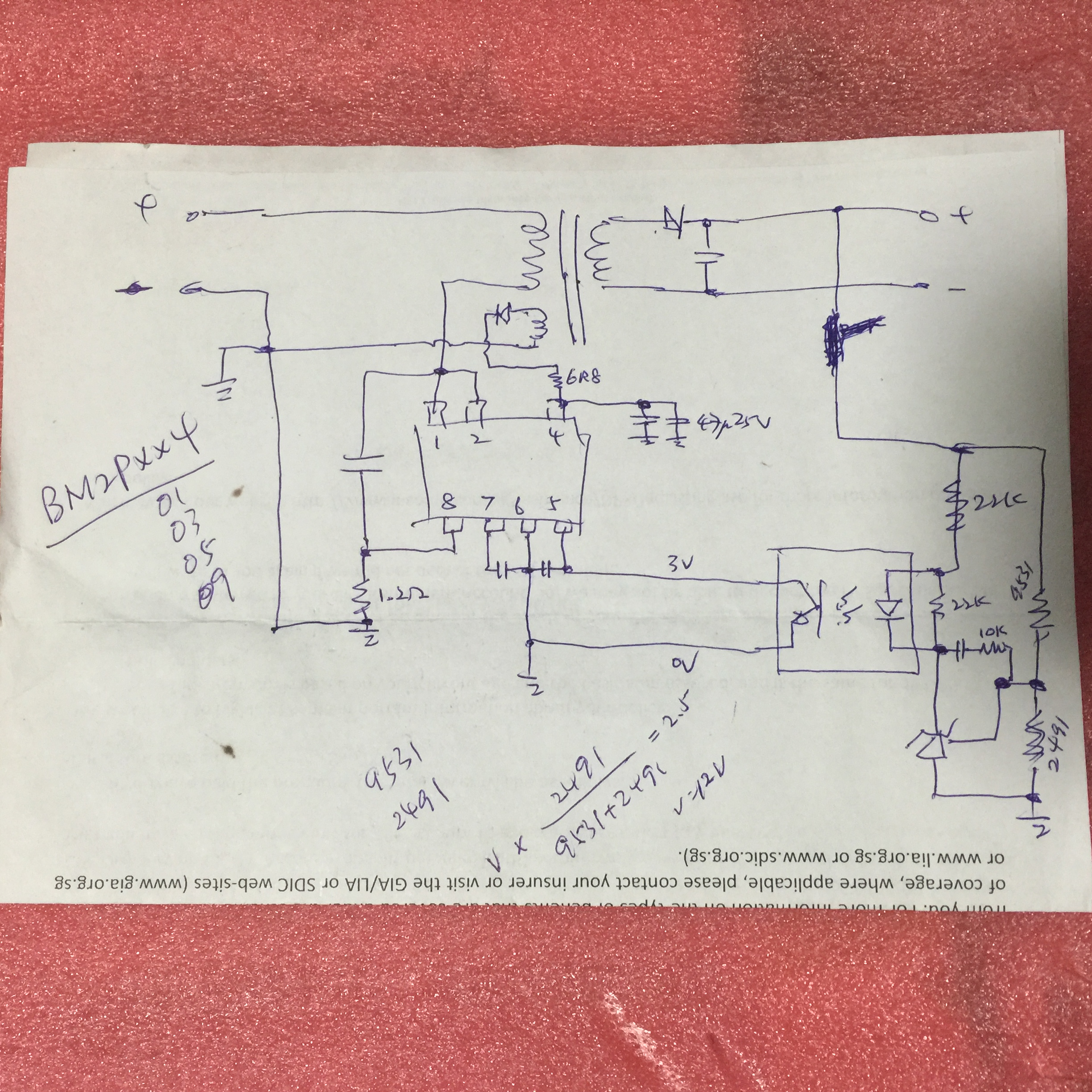
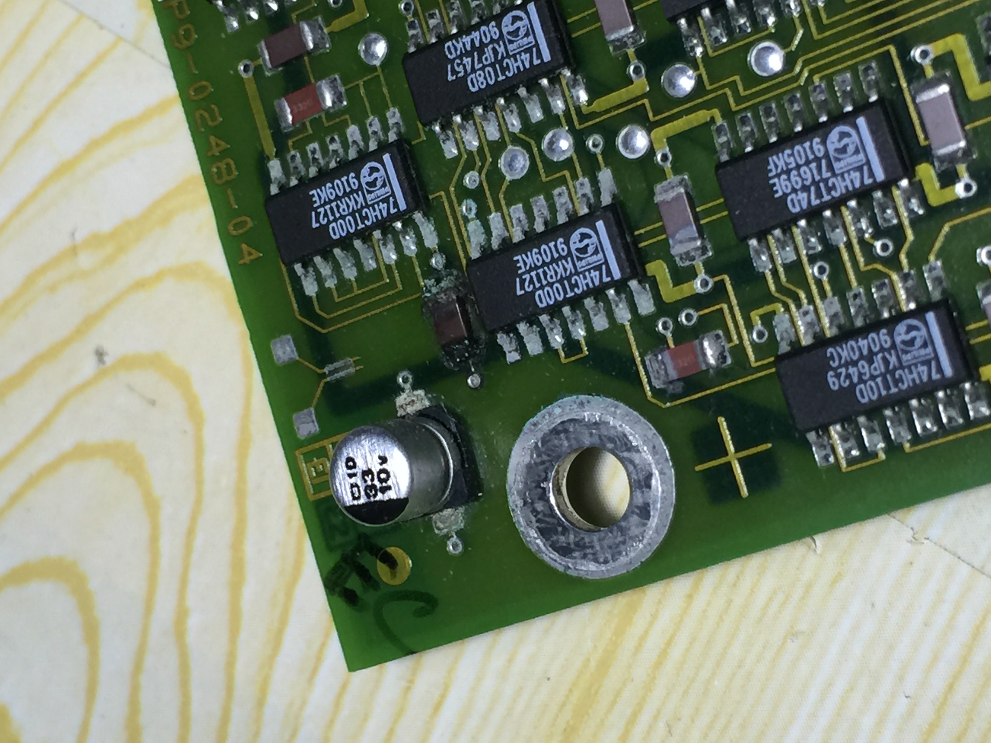
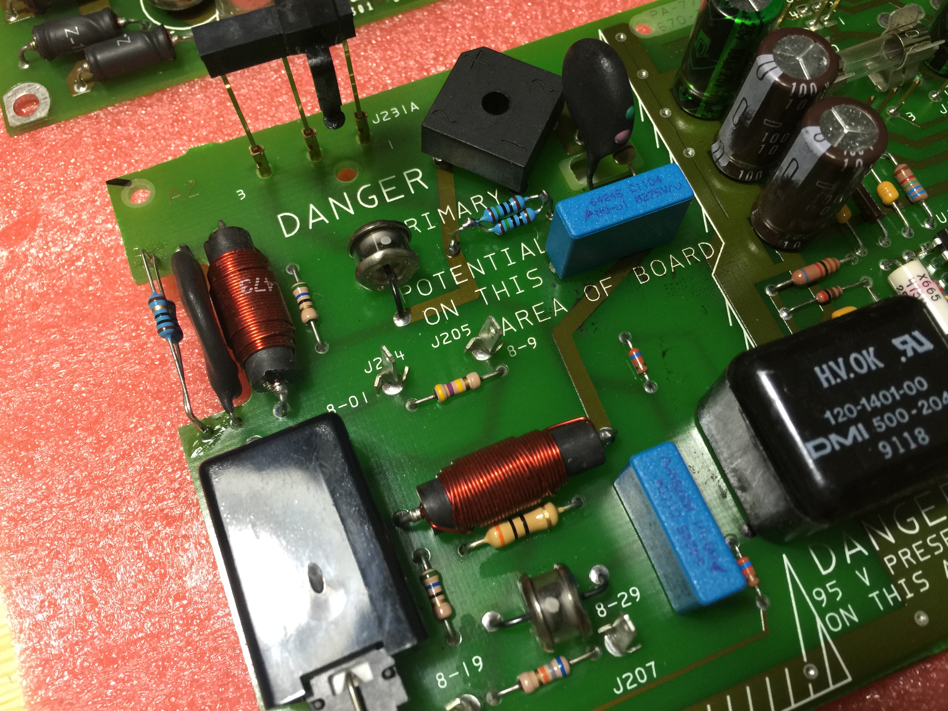
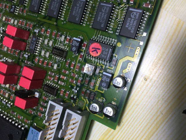
The first suspect is the high voltage board defective and I open it and do a check on the high voltage board switching transistor and everything looks fine. Also I can get about 65k switching frequency at the switch mode power supply. After looking around, I see there is a “G Bias” pot on the high voltage board and then I turn it clockwise and see some display DOT on the screen. The scope wordings of time base and input attention can be seen also. Thus I reboot it and see a “Step 05 fail 44” error on the screen. After checking the service manual it point to the DAC on the control board and thus I look at it again. Oh I find the leaking SMD capacitors with corrosion in its surrounding components.
It can be seen that the components surrounding the three E-cap are with corrosion solder join! So in totally changed all 4 SMD e-caps on the control board as the other corner also have one more leakage e-cap.
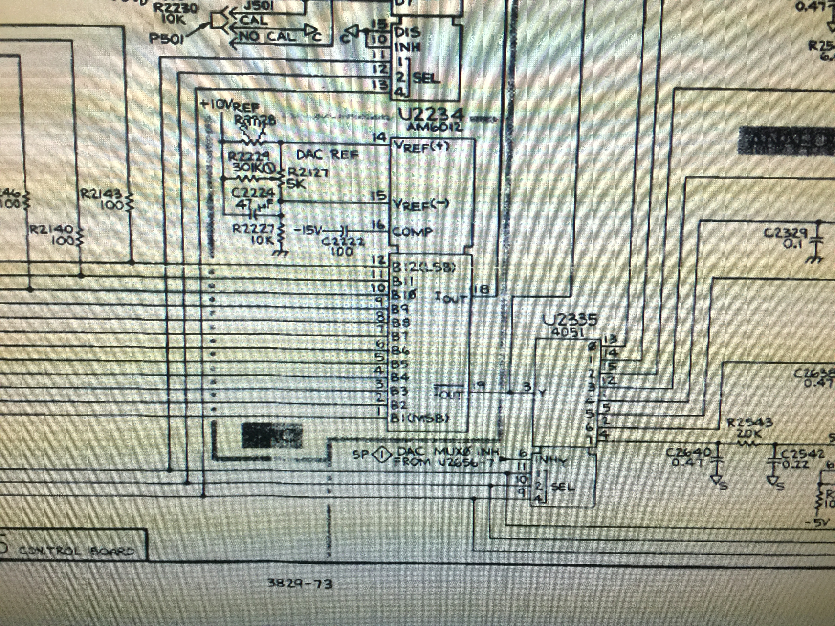
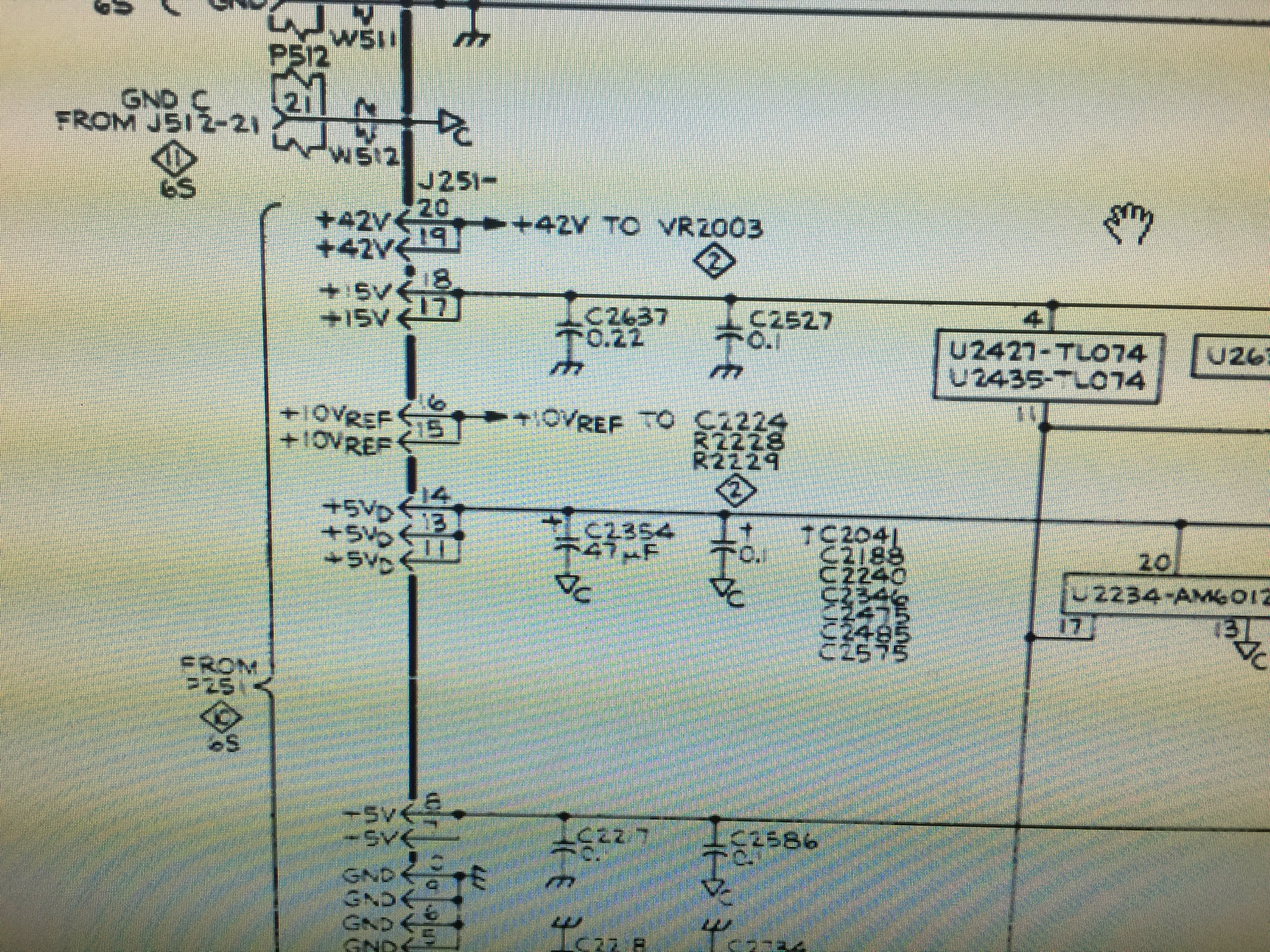
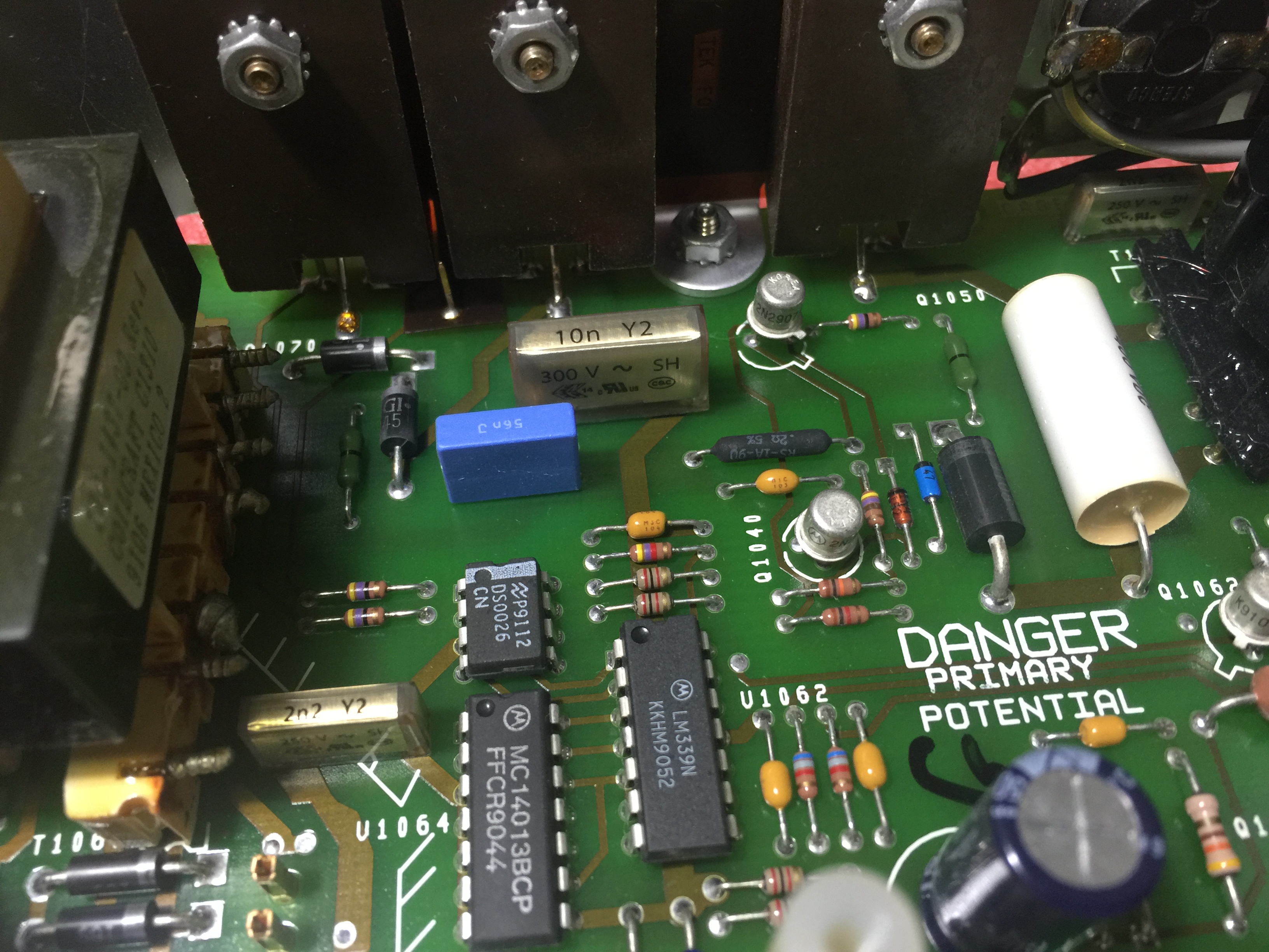
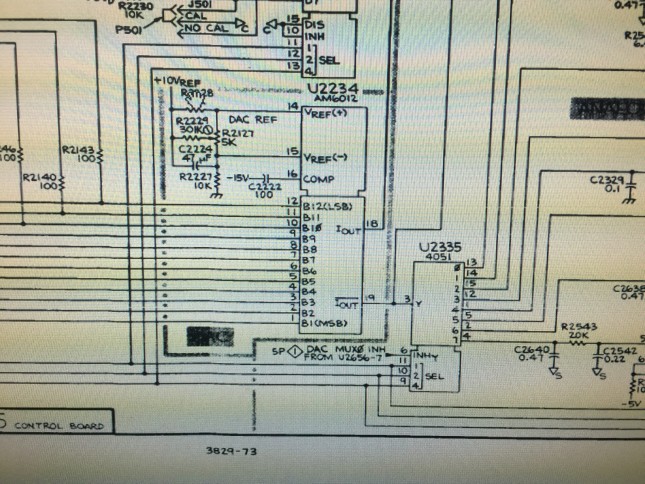
After changed the 4 caps, I put back the board and power on the set but the failure symptom is still same step 05 fail 44!!! So I probe around the DAC chip and check the Vref 10V at pins 14 and pin 15. The voltage is really low and close to 0 volt.
So I started to check the components around the DAC U2234 and later find out that the resistor R2228 10k is open circuit. I replace it with another one smd resistor and after that I power up the set and it works again!
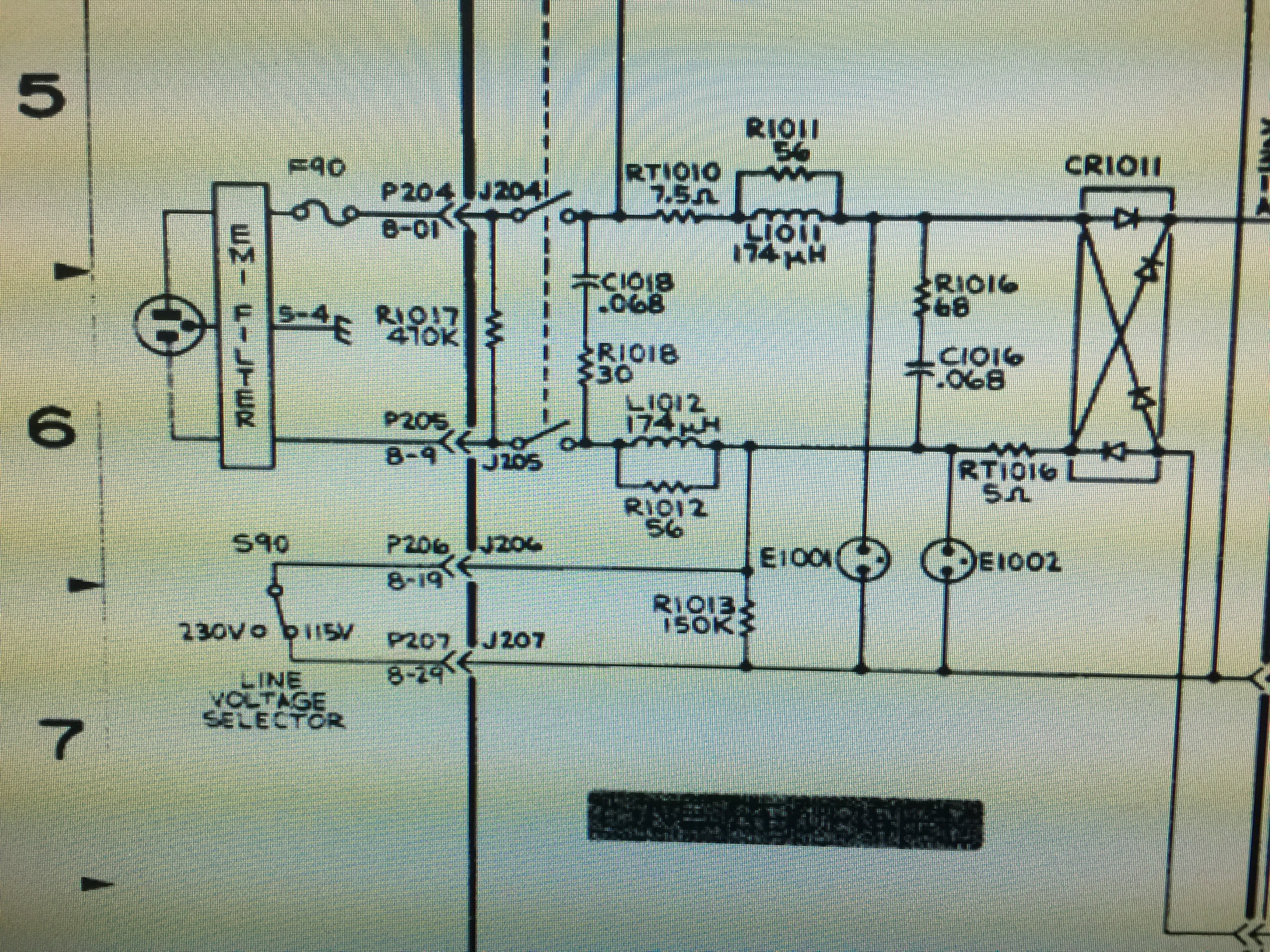
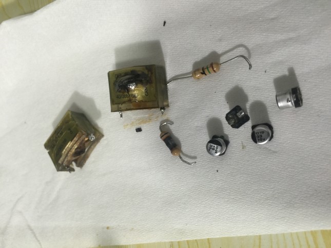
I burn in the set for about 15 mins and then I start to smell something from the scope and of course power off it immediately. Open up and found the line filter caps (RIFA) brands are all burnt together with two more resistors.
C1018, R1018, C1016, R1010 (parallel with RT1010; 15 ohm not on schematic) were all burnt of open circuits. Later I also find three more Rifa capacitors on the other PCB (2200pf and 10nF 250v ~ is also crack a bit on the body. I take them out and all the 2200 pf caps are with very low value of about 100pf! Thus I order them from element14 and they arrive after 3 days. For the 0.068u 250V~ cap, I use on hand 0.1uf 250V~ cap to replace them (blue color on the picture). After put back, everything works fine. I have brought this 25 years old scope back to life!
I also note that there are many same scope 2445 or 2445B with similar failure of step 05 fail 44. I hope this information can help some of the people to repair their scope.


Related Images: