FET Audio | Hi-End Audio & Electronics DIY Electronics & Repair

February 13, 2022

D1V2 + Zen I/V PCB – Aka D1 Clone

Filed under: DAC — Spencer @ 11:38 am

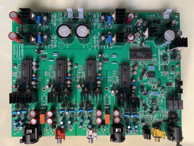
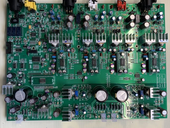
Completed to re-design my old D1V3.3 or D1 clone pcb as below:  Name it D1V2 + Zen I/V.  Please write to me if you are interested in the PCB.  No kit offer!  Full assembly Boards with limited supply only.

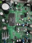
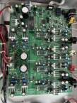
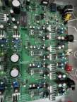
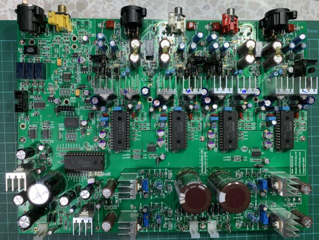
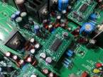
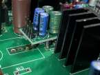
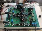
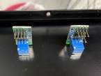
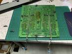
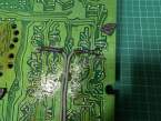
Totally I have made 3 versions of boards for testing – V17, V28 and V30.  The photos of each version is as below in sequence.

The board can use DAC – PCM63, PCM1702 and PCM1704.  Note PCM170x need to use a converter board as in second picture.  For digital filter, it can use SM5842, SM5843, SM5813, DF1700, PMD100, DF1704, DF1706 etc…  Digital receiver is WM8804 with excellent jitter performance.  More details in the reference manual below.

Compare to D1V33, it is much better in sound stage, imaging, resolution and details.  It still remain the analogy sound of smoothness and best vocal DAC when PCM63 is used.  When DF1704 and PCM1704 is used, the input is set to 16-24 bit digital input mode and output of DF is set to 24 bit mode.  The resolution is found better than PCM63 a bit but remain the smoothness of R-2R DAC sound.

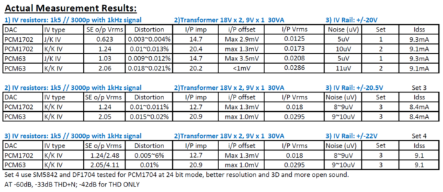
Two versions if Zen IV are tested – J/K and K/K.  Here is the summary of measured results : IV resistors & capacitors and Rail comparison table_v30

Conclusion is to use the KK IV + KK Buffer – 2SK369 or 2SK363 is the optimum design choice using 20V rails.  Nelson Pass original Zen IV using JK IV is having too weak output level at 30V rails.  Also J74 is not available easily with reasonable cost.

Reference Manuals:

D1V2_ZenIV Manual v30.1_ALL

D1V2_ZenIV Manual v28.3_all

D1V2_ZenIV_Manual_V17

Digital filter setting table (apply to all Version boards): DIGITAL FILTER PIN CROSS REFERENCE SM5842_V30.4

Related Images:

January 30, 2022

D1V33 + Zen I/V re-visit

Filed under: DAC — Spencer @ 10:47 pm

The Zen I/V was posted by Mr. Nelson Pass back in 2010.  I have not enough time to try that due to my work location change and far away from my equipment.  I am back home since 2021 and now it is time to try out the Zen I/V.  Below is the photos of the Zen IV that I put on the D1V33 board and so far the result is very positive. The distortion for SE measurement can be down to 0.002% to 0.004%, in fact that is the distortion spec of the DAC chip.  Here is the information sharing for anyone interested to comment.

  1. Rail voltage is only +/-20V as it is the limit of the current D1V33 board default supply. 
  2. Use Drain resistor of 1.5k ohm due to limit of the rail voltage and thus give a Vd about 7V for jfet Idss of about 8mA.  This is compromise due to Rail voltage max at 20V.
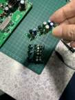
  3. Use daughter boards to put on top of original jfet IV locations.  Since the pins for supply, input and output are not the same, thus I have to design 4 similar boards with different locations of the pins.  The boards are names #1 ~ #4 for identification.  Daughter Board is connected to main board via pins, some holes are not really on top and thus the pin has to be soldered a bit tilted (best locations of pins).
  4. Emitter follower is added to the Zen I/V with a pair of transistors to buffer the output to have lower output impedance.  The distortion so far do not see any degrade in readings.  In fact jfets pairs can be used but it will increase the cost!
  5. SMD resistors 1206 or MELF 1/4 W and capacitors 0805 are used on top and bottom of boards to make the board as small as possible.
  6. Tough job is to remove the original Jfet IV parts on the main board and it is helped by a de-solder station make by YiHua 948 (about US$60).  SMD part is soldered with hot air gun also YiHua 8786D 2-in-1 station (about US%65).  Really handy tools and cheap!
  7. I still left some pcbs and thus those interested, I can send to them with cost of SGD$20 for each set (include paypal and shipping cost).  Sorry I do not have any more K170/J74 match pairs for sell!

My version of Zen I/V circuit: D1_V2_2_ZenIV_ckt

3D view of the Zen I/V board: D1_V2_2_ZenIV_3D

Related Images:

October 22, 2021

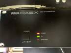
Yamaha DA8X convert from Y2 to AES digital input

Filed under: DAC,Pro Audio — Spencer @ 10:15 pm

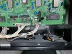
Total I brought two of these DA8X but I never have chance to hear the music from it.  Here is what I do to make it works:

Details modification procedure (New V4): Yamaha DA8X Modification from Y2 input to AES input v4

Data sheet: YM3436

Draft: DA8X draft notes

DA8X service manual: https://www.synthxl.com/yamaha-da-8x/

Bourns Pot: Bourns 10kA 1874875

Related Images:

February 16, 2021

Re-Life to D1 PCM63 DAC

Filed under: DAC,Gallery — Spencer @ 2:12 pm

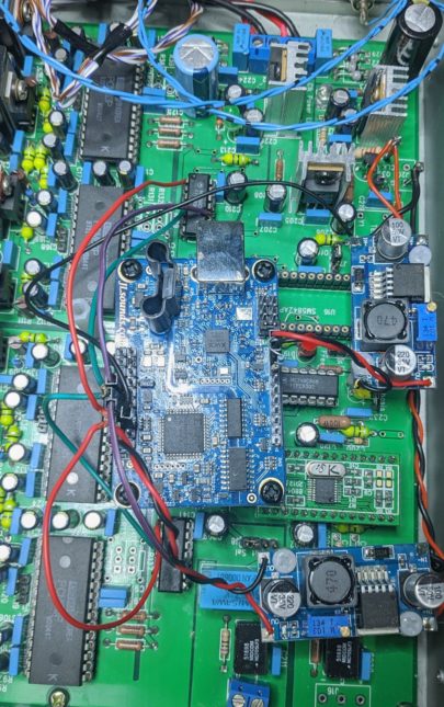
With the work of 1 year away from home, I am back to Singapore and thus able to be with my old hobbies – DIY audio. During this time, I was approached by a DIYer about the modification of the D1V2 (http://www.fetaudio.com/archives/23) board to use USB input for network audio. After some discussion, the DIYer is able to make it work and here I share the details of the modifications of the USB to PCM63 DAC with permission. I keep all the original text of the modifications and only added few comments in the text.

Picture of the Modifications:

Related Images:

May 11, 2014

F5T Pre-amp + FDA-2A AD1955 DAC in one box

Filed under: DAC,Pass Amplifiers — Spencer @ 12:52 pm

This is a pre-amp plus a FDA-2A in one box.  It was built in year 2012.  I use a old Yamaha DA8X box to house eveythings insides.  See the pdf files at bottom for details.

DAC:

FDA-2A with USB, Optical and AES digital input.  Push button for digital input selection at the front panel.

DAC direct output is available in RCA sockets.

F5T Pre-amp:

Alps volume control from DAC output and note that there is no other analogy input for the preamp.

The pre-amp is based on Nelson Pass F5T power amp design and striped down to only one pair mosfet and lower bias current at about 200mA.  Supplier voltage is at about +/-23V with a small transformer.  Power mosfet is using Toshiba J200 / K1529 pair and casing is acted as the heatsink of power mosfet.

A headphone jack is connected in parallel with the pre-amp RCA sockets.  It can drive most headphones due to sufficient high bias of the power mosfets.

DSC_0045s

Details refer to this pdf file: F5T-Pre_DAC

Enjoy!


Related Images:

Older Posts »

Powered by WordPress